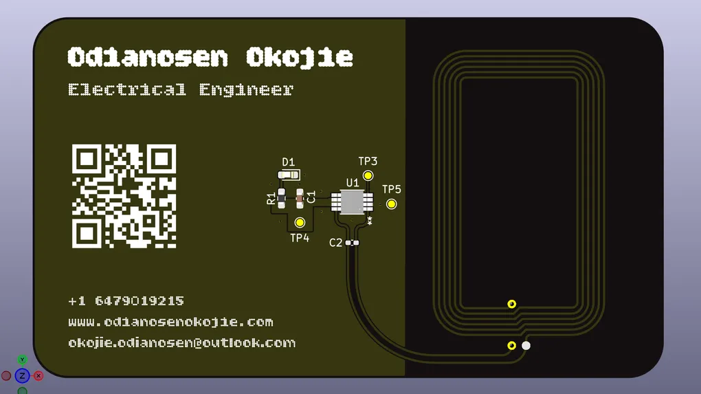
NFC Business Card
View repository →Overview
I’ve been meaning to do more personal projects and design more PCBs outside of work. In the past couple months, I saw a lot of people making PCB business cards and thought it might be a cute thing to make.
Additionally, I used it as an introductory demo for the first session of Netca, a hardware workshop series aimed at a mixed technical and non-technical audience. The goal was to design something simple where you could immediately see the effect: tap the card against a phone, and be able to share links/contact details.
Spec Sheet
- 2 layer PCB
- 0.8 mm thick
- NFC chip
- NXP Class 5 NFC Antenna
Key Terms
A short glossary for anyone following along who isn’t already fluent in PCB/RF shorthand:
- NFC (Near Field Communication) — short-range wireless communication that operates a at a specific frequency (13.56MHz), used here to let a phone read the card passively, with no battery.
- Silkscreen — the printed ink layer that carries text, graphics, and reference labels on a board’s surface.
- Solder mask — the colored protective coating over the copper layers (black in this context)
- Refdes (reference designator) — the small labels (R1, C1, U1, D1…) identifying individual components on the silkscreen.
- Gerbers — the standard set of manufacturing files a fab uses to actually produce the board.
Design notes
Antenna and tuning. The antenna replicates NXP’s AN11276 Class 5 reference design. Lots of details regarding antenna design guidelines from the an11276-ntag-antenna-design-guide. Unfortunately, I was unable to get the necessary footprint file I needed to put into KiCAD, just the gerber files in Eagle. So I opened up the Gerber files in KiCAD, deleted unnecessary parts of the reference design, and copied the antenna tracks into a blank PCB. Then I used AI to analyze the file and spit out a footprint file that matched and did final touches regarding pads and vias manually.
Logo placement. A concentric-infinity mark, supplied as clean vector SVG, went in via KiCad’s native File → Import → Graphics .
Surface finish. The card is meant to be carried and handled for a long time, and it has intentionally exposed test points (TP3, TP4, TP5) that you can probe during an energy-harvesting demo. Therefore using something like a thin, easily-worn coating such as OSP falls short, plus I preferred the durable gold finish of ENIG compared to silver.
WIP
Result
TBD